The worldwide embrace of smartphones and tablets with thin form factors is driving demand for semiconductor devices to be smaller and more highly integrated. Extremely precise mold thickness management is necessary for these cutting-edge semiconductor processes. However, quality managementin the molding process has been challenged by the fact that non-destructive mold thickness measurement tools were not available, meaning that engineers must extract individual device samples during the trim and form process and inspect them by microscope.
Advantest's TS9000 MTA Option solves these issues by utilizing terahertz waves to measure mold thickness non-destructively, rapidly, and with a high degree of precision. The system's high throughput enables users to test large volumes of samples and readily grasp the mold thickness distribution of entire lots. For the first time, users can inspect mold thickness during volume production.
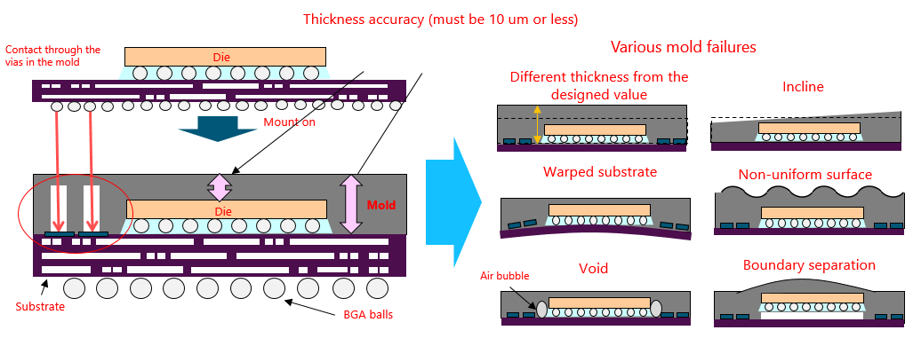
Mold Thickness Inspection with Mounted Chips
TS9000 MTA detects faulty mold on the strip to eliminate failures when mounting.
Points for mold quality management in each layer of 3D mounted chips
- For PoP mounting, the thickness and uniformity need to be as designed when making vias in the mold.
- Before mounting, the mold status in each layer must be ascertained to improve yields when mounting.
Analysis mechanism of TS9000 MTA option
The TS9000 MTA Option places the semiconductor devices to be measured on the measurement unit on the XY stage. It rapidly measures multiple "measurement points" and analyses the mold thickness distribution. The measurement unit supports devices in various formats, including wafers, strips and trays as well as individual chips, using industry standard JEDEC trays or customer trays.
Mold Thickness Analysis With Terahertz Technology
The TS9000 MTA Option generates terahertz pulses, which are partially reflected by the surface of the package, and partially by layers within the package. Their echoes are detected, and the time difference between the return of the signals is computed, allowing the system to analyze the thickness of the mold.