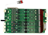
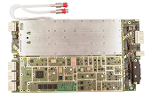
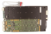
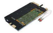
Direct Probe™
High-performance, multi-site functional testing now possible at wafer probe
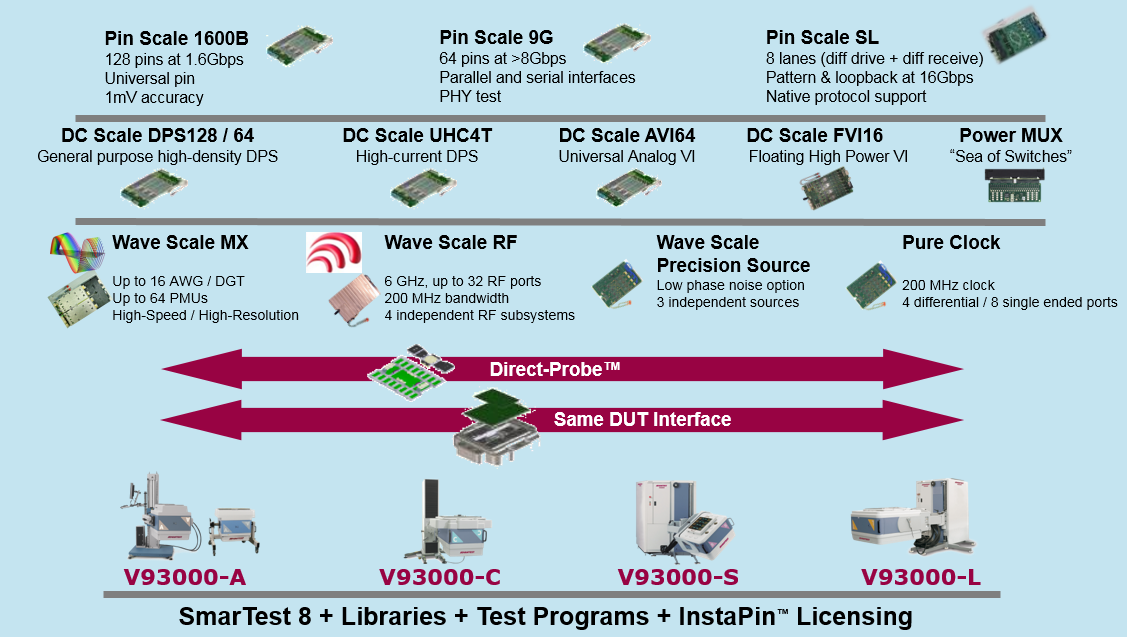
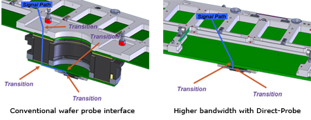
Advantest's V93000 Direct Probe™solution reduces the length and number of signal path transitions between tester and probe card enabling the industry's highest test performance to now be brought to wireless, WLCSP, MPU and GPU devices at wafer probe.
Working closely with leading probe card manufacturers, Advantest has successfully overcome traditional barriers to delivering high performance test at wafer probe. Advantest's Direct Probe™ reduces the length and number of signal-path connections between tester pin electronics and probe points, significantly improving signal integrity for device testing. With higher quality signals, the control and performance needed for accurate stimulation and full functional testing of digital, mixed-signal and RF devices directly on the wafer is possible.
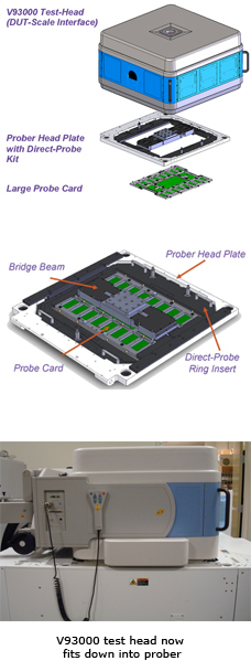
Direct Probe™ utilizes an innovative probe card based on a single load board that directly incorporates the probe points. The single load board can leverage existing final test designs and can be shared between wafer probe and final test, reducing hardware development time and hardware cost.
Direct Probe™ is mechanically designed and engineered for contact force management and with the planarity to support large surfaces and high pin counts at wafer test. The result: excellent mechanical and electrical contact is assured.
- With Advantest's V93000 Direct Probe solution, manufacturers can now take a major step forward toward complete high performance functional testing at wafer probe and significantly lower cost of test
- Maximum test resource utilization, high parallelism and high throughput for lowest cost of test
- Shorter hardware development time and cost due to innovative probe card design
- High-performance signal integrity from tester pin electronics to probe tip
- Mechanically designed for contact force management and planarity to support large surfaces and high pin counts at wafer test
Introducing Direct Probe 2.0
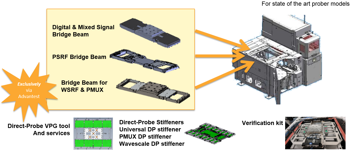
Advantest now provides the overhauled Direct-Probe infrastructure (bridge beam, stiffeners, alignment & verification tool) for state-of-the-art prober models directly.
Advantest’s bridge beams provide:
- Certified tolerances matching with Advantest made probe card stiffeners for trouble free operation
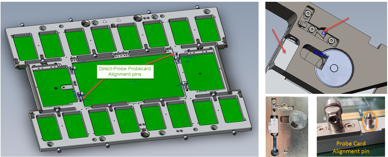
- Probe card cam lock interlock with probe cards which eliminates realignment need after cleaning interval for superior probe cell efficiency
- Controlled and specified deflection characteristics for superior contacting robustness even at very high probe counts (50.000)
The Advantest bridge beams are specifically designed to match all application areas, featuring cut outs to provide the required instrument space, so that the new front-end modules can access the DUT interface board / probe card. (Cut outs impact deflection/rigidity properties)
Features&Benefits
| Feature | Benefit |
| Scalable support of digital, mixed-signal and RF devices | Ideal for wireless, WLCSP, MPU and GPU devices; Maximum test resource utilization for greatest return on capital investment |
| Test head in direct contact with probe card | High-performance signal integrity for functional test at wafer stage |
| High multi-site capability | High parallelism and throughput to lower cost of test |
| Contact force up to 400KG with superior planarity | Excellent contact quality for large die and high pin count devices |
| Superior probe card interlock | Superior x/y repeatability after cleaning step.
Interlock eliminates the need for probe card alignment after probe head cleaning |
| High rigidity for different application areas | WaveScale RF/PMUX beam
General purpose/digital beam
PortScale RF beam |
Detailed Benefits
Highest performance for high-volume manufacturing, multi-site probe test of digital, mixed-signal and RF devices at wafer stage
- Enables probe test of high pin count MPU/GPU devices requiring high digital performance and high current contacting
- Consumer audio/video, mixed-signal and RF devices that are rapidly moving to wafer-level chip scale packaging (WLCSP) and require high performance probe test
Maximum test resource utilization, high parallelism and high throughput for lowest cost of test
With greater multi-site testing, reduced index times (<1s) and faster test times, manufacturers can achieve the high throughput needed to drive down cost of test.
Innovative probe card design, reducing hardware cost and hardware design time
V93000 Direct Probe™ 's innovative probe card design, places the probe assembly directly on the load board, improving test performance and reducing hardware cost and hardware design time from design to production.
High-performance signal integrity from tester pin electronics to probe tip
The current industry standard for wafer prober interface (Pogo Tower) degrades the signal quality because the signal must pass through multiple transition points and a distance of 4 to 5 inches. V93000 Direct Probe™ interfaces the test head directly with the probe assembly, reducing the length and number of signal path transitions, maintaining signal integrity.
Mechanically designed for contact force management and planarity to support large surfaces and high pin counts at wafer test
V93000 Direct Probe™ addresses all major contacting challenges (pad probe, Flip Chip, TSV(Through Silicon Vias) and WLCSP) by supporting contact force up to 400 kg and maintaining planarity (1mm over 44,000mm2) for excellent mechanical and electrical contact quality for large die sizes and in high pin count devices such as with MPUs and GPUs.
Probe card cam lock interlock with probe cards which eliminates realignment need after cleaning interval for superior probe cell efficiency
During card clamp operation, Direct-Probe Bridge Beam pushes and holds probe card alignment pins to the datum point, and constraints XY card movement.
