V93000 SoC / Smart Scale
SoC Test System
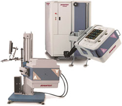
The requirements of today's SoC/SIP industry for ever higher speeds, performance and pin counts means that test systems must offer greater functionality while maintaining low cost of test. The scalable platform architecture of the Advantest V93000 combines the highest speed digital test, precision analog and RF measurement into a single test system. With the majority of the functionality tightly integrated into the system's test head, the platform offers superior speed, performance analog as well as the lowest noise floor. Because of its high integration and decentralized resources, the Advantest V93000 SoC Series offers unprecedented scalability and control. Its modular design makes it easy to extend the system with new modules and instrumentation, as your test needs change.
Features
Broad application
Coverage from simple low end devices to the most complex high end products requiring the full suite of capabilities:
dc, digital, analog and RF.
Maximum flexibility and scalability
By supporting any combination of the instruments in any of the test heads.
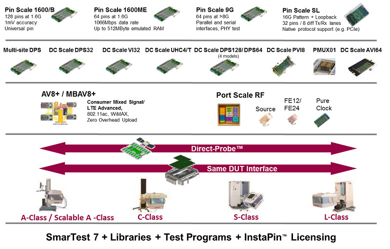
V93000 Smart Scale
Compatibility across the whole platform
By using the same hardware architecture, same test programs, same load boards and same docking, enabling new capabilities to be added over time.
Capabilities when and where they are needed
Through floating licenses which can be shared within a tester or between testers, to enable additional capabilities while optimizing investments.
Maximum investment protection
Through the continuous evolution of the platform, maximizing reuse in the engineering community knowledge base and extending the life time of the tester.
Staying focused on the single scalable platform strategy, Advantest has developed a significant installed base of V93000 test systems in both engineering and high volume manufacturing, gaining acceptance at the leading IDMs, foundries, design houses and OSATs throughout the world.
Solution
- • Versatile Digital Solution:
The V93000 Versatile Digital solution provides coverage of the "all digital" space from structural wafer sort to high end characterization test, from consumer to high end all on a single platform providing our customers the benefit of maximum versatility. - • Wireless/RF Solution:
The V93000 Wireless/RF solution provides highest test efficiency and minimum cost-of-test, with up to 96 ports, octal-site with highest multi-site efficiency. - • Consumer SoC Solution:
The V93000 Consumer SoC Solution is the best way to achieve low cost-of-test while accurately overcoming the unique mixed signal testing challenges of the latest consumer device SoCs. - • Power/Analog Solution:
Versatile Digital Solution
Coverage of the "all digital" space from structural wafer sort to high end characterization test, from consumer space to high end all on one platform providing our customers the benefit of maximum versatility.
Industry Challenges
The drive for more functions per die, the drive for power reduction to enable ever longer battery lifetime of mobile devices drives technology nodes. Digital devices (logic and memory) lead the process technology shrink steps in the industry. Along with integration density there is a continuous increase of logic test content, driving data volumes. Very high speed I/O technology, SerDes based (such as PCIe, HDMI.. ) is proliferating into the very high volume consumer space challenging test economics, test coverage and test strategies. New technologies consistently come with new fail mechanisms, such that advanced silicon debug becomes an integral necessity in the race to market. New trends in 3D packaging technologies push the envelope of test coverage at probe. Seamless integration with the design tools, full automation of the design to test and test back to design flow and process are key to success.
The V93000 Versatile Digital Solution
The V93000 digital test solutions are based upon Advantest's proven per-pin architecture, enabling a broad variety of capabilities for the core digital test cases. Whether you need to address very high node counts, address a high degree of parallelism and multisite efficiency, address large scan data volumes, support sophisticated power delivery or explore very high speeds or timing accuracy, the V93000 provides solutions across the entire space in one go.
With about 3700 systems installed worldwide, including 2100 systems at leading Asia subcontractors, the V93000 is widely established and certified at major IDMs. The platform has become the all purpose reference platform.
Superior cross platform compatibility allows our upstream customers to choose from state of the art latest systems or load the same base program on the large fleet of legacy V93000 system for the more mature products, thus picking optimum cost of test operating points. For the OSATs the cross generation compatibility means maximum investment protection, optimum reuse of resources and a high degree of flexibility for load balancing within the fleet.
The uncompromised per-pin architecture of the V93000 resources as deployed in the SmartScale series cards results in a number of key benefits and assets for the "heavy digital" application domain:
- • All per-pin DC resources leading maximum parallelism
- • Per-pin TMU addressing the pervasive use of local PLL-based time domain synthesis avoiding no special resources and routing
- • Per-pin sequencing enabling flexible I/O port assignments and concurrent execution of multi domain functions
- • Versatility and scalability of power supply sources to 100's of mili-amps with per resource integrated measurement capability
- • Flexible vector memory architecture and licensing options enabling a broad mix of deep scan to high speed functional assignment
- • Leading edge performance cards augment the offering of general purpose capability all the way up the 12.8 GB/s with Pin Scale SL
Wireless/RF Solution
RF is ubiquitous, found in cell phones, satellite-based navigation, tuners, set-top boxes, WLAN, Bluetooth, FM Radio, UWB, PCs and laptops. In the past, RF parts were separate, individual "jelly bean" parts. Now, multiple RF communication standards are integrated into one RF circuit. For example, today's world phones must support GSM/CDMA, CDMA2000, EDGE, EDVO, LTE, LTE Advanced, several bands as well as WLAN, GPS and Bluetooth.
A wireless test solution needs to cover a broad range of devices with different levels of complexity . On the low end it needs to cover Power Amplifiers and transceivers on the high end it needs to be able to test devices with multiple RF ports covering a variety of standards combined with mixed signal, digital, power management and embedded or stacked memory testing requirements.
V93000 Wireless Test Solution - Port Scale RF
The V93000 offers one single platform to cover the broad range of requirements to test the variety of wireless devices thus enabling unprecedented asset utilization and manufacturing flexibility. This combined with lowest cost of tests results in a widespread market acceptance of the V93000 RF solution and sets a new standard for testing next generation RF devices.
Lowest Cost-of-Test with Scalable, Parallel RF Test
Test cell throughput and multi-site efficiency have the highest impact on cost-of test (COT). The V93000 Port Scale RF architecture makes key contributions in several dimensions:
- • High multisite through # of RF ports
Port Scale RF can be configured with up to 96 RF ports to handle the increasing complexity of multiple radios integrated into a single device, and to enable multi-site testing of these highly integrated devices while maintaining the ability to scale down for low-cost testing of low-integration RF devices. - • Multisite efficiency
With its parallel RF test capability, Port Scale RF easily doubles the RF multi-site efficiency of previous generation RF ATE, delivering greater than 95% efficiency. - • Industry leading single site throughput
Previous generations of RF SoC ATE offered one RF receiver multiplexed to many RF ports, resulting in inefficient serial multi-site test. Scale RF offers up to 8 parallel RF receivers for true parallel test, so four devices can be tested in parallel AND two RF ports on each device can be tested concurrently, or up to 8 devices can be tested in parallel. Further parallelism is introduced through hidden upload, multithreading for parallel upload and data processing and through concurrent test. With the hidden upload feature testing can continue while large amounts of data are transferred to the workstation for processing. In addition data processing can be done in parallel with the data upload using multithreading. With concurrent test it is even possible to test different cores in parallel (e.g RF and digital). In addition to parallelism the throughput is further improved by fast frequency and power level changes and with the industry's lowest noise floor (-161 dBm/Hz) resulting in fewer acquisitions and less averaging.
Direct Probe™High performance, high quality test at wafer level through Direct Probe™ solution
WLCSP require test coverage of final test at probe to enable “known good die” testing. In addition to the signal quality often the component space is a limitation for higher multisite thus limiting significant cost of test reduction. With it's breakthrough Direct Probe™ probe card interface technology the V93000 offers 4 times the component space on the probe card with optimal signal integrity to allow “known good die” testing with higher multisite already at probe.
Fastest Time to Market
Implementing the demodulation for the ever growing number of standards is very time consuming. To significantly speed up test program development and with this reduce the time to market the V93000 provides a comprehensive ready to use demodulation library which covers all major standards and which is continuously extended. Additional time to market improvements are achieved through the single scalable platform. Engineering time is reduced through test program reuse. Training needs are limited due to a single, familiar test system.
Unprecedented asset utilization and manufacturing flexibility through single platform
The Advantest V93000 SoC Test Platform offers the widest application coverage in the industry, handling the latest generation devices that contain, for example, hi-fi quality audio, video capability, RF and high-speed digital interfaces. The wide application coverage results in unprecedented asset utilization and manufacturing flexibility. Additional efficiencies are gained from the consistent software platform, the same hardware modules from one system to the next (digital, analog, RF, etc.) in a choice of compact, small or large testhead, DUT board reuse and use of the same docking hardware and positioning, which results in a consistent prober and handler setup on the test floor.
Consumer SoC Solution
As silicon has become a commodity in the 21st century, chip manufacturers are forced to respond to cost pressures by taking measures such as maximizing their use of IP, integrating more functionality into smaller silicon geometries and increasing quality while significantly driving down the cost of test.
V93000 SoC Test Solution
The V93000 is the only single scalable platform ATE offering solutions from entry level consumer devices to the most complex high end integrated SoC requiring the full suite of capabilities: dc, digital, high speed digital, analog and RF.
The scalability of the V93000 infrastructure enables cost optimization of configurations and further cost of test reductions can be achieved by:
- • Optimized throughput with zero overhead background upload and background calculations enabled by SmartCalc
- • Very high multi-site efficiency in terms of both throughput and tester resource utilization enabled by Advantest's unique tester per-pin architecture
Cost optimization is not only achieved at the tester infrastructure level, but also at card level through the modular design approach maximizing ROI down to the per-pin level:
- • InstaPin licenses allow the data rate and memory depth of digital channels to be scaled to match the requirements of the target application, minimizing the cost of carrying unused tester resources.
- • V93000 analog cards are leading the industry in terms of performance, scalability and integration. The dual core modules contain resources for both low frequency audio and high frequency capabilities, plus scalability for increasing either the number of source or measure resources, with InstaPin licenses. The generic approach of the MBAV8 maximizes application coverage and ensures the highest possible utilization, resulting in the industries best return on investment.
Proven in both engineering and HVM, V93000 solutions are installed in major IDM, design houses and subcontract manufacturers testing a whole range of devices from cost driven digital TV chips through to fully integrated single chip SoC for mobile phones.
Power/Analog Solution
The new PVI8 floating power source extends the capabilities of its market-leading V93000 test platform for high-voltage and high-current testing of embedded power devices.
This enhancement gives the V93000 sufficient power and enough analog and digital channels on a single platform to conduct highly parallel, cost-efficient testing of embedded power ICs.
Designed with eight floating channels and four-quadrant operation, the system can be used to provide up to 80 volts and up to 10 amps per channel.
The Ultimate Choice in Scalability
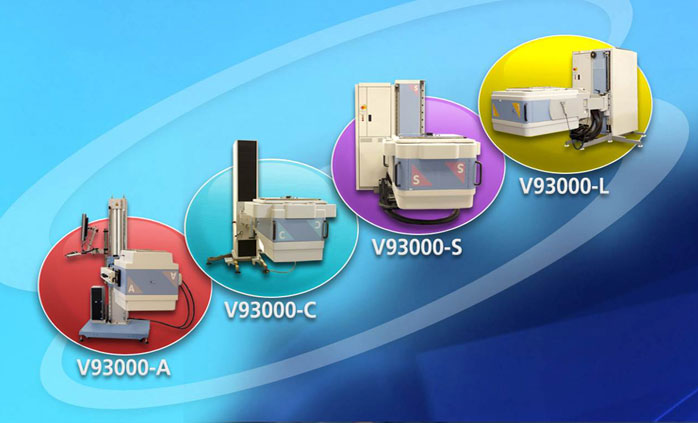
The V93000 Smart Scale Generation extends the V93000 for the broadest device coverage in a single platform with a full range of compatible tester classes (from the smallest A-class to the largest L-class) to maximize your return-on-investment.
New Cards, New Capabilities
The V93000 Smart Scale Generation introduces cards with new capabilities that efficiently increase test coverage, improve time-to-market and deliver superior test economics:
- Industry-leading digital performance and high-speed I/O flexibility
- System-Like Stress Test
- Protocol-engine-per-pin
- Real-time memory emulation
- SmartLoop™
- Enhanced SmarTest™ software functionality
Pin Scale 1600 Digital Card
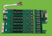
The Pin Scale 1600 digital channel card brings a new dimension in test flexibility. Per pin capabilities such as individual clock domain, high accuracy DC and industry-leading digital performance are expanded with the Pin Scale 1600.
Pin Scale 9G Digital Card
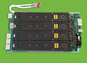
The Pin Scale 9G is the only fully integrated, high-speed, digital instrument covering the entire range from DC up to 8 Gigabits per second. With its flexibility, the Pin Scale 9G can test any combination of parallel or serial, single ended or differential, and uni- or bi-directional interfaces.
Pin Scale SL High Speed Card
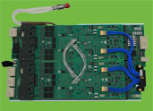
Pin Scale SL extends the leadership in high speed ATE instrumentation into the 12.8/16G domain. Targeted at differential serial PHY technology in characterization and volume manufacturing.
MB-AV8 PLUS Analog Card
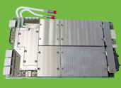
MB-AV8 PLUS expands the real-time analog bandwidth to cover emerging applications such as LTE Advanced. It improves throughput while maintaining compatibility with the established MBAV8 instrument.
DC Scale DPS128
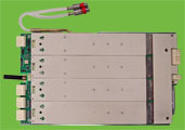
High density DPS for massive multi-site applications - extending the power supply versatility of the V93000. Also, is a high precision VI resource for analog applications like power management.
DC Scale PVI8
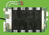
The eight-channel PVI8 floating power source provides the capability to conduct highly parallel, cost-efficient test of embedded power devices. Each channel can provide up to ±80V and ±10 amps. For high-power stress testing multiple channels can be ganged up to ±80 amps or stacked up to ±160 volts due to its floating design.
Setting the Standard in Test
Smart Test, Smart ATE, Smart Scale. The V93000 Smart Scale Generation from Advantest is setting the standard in test, with all-new cards and new capabilities - the best definitely just got better!
Direct Probe™
High-performance, multi-site functional testing now possible at wafer probe
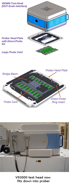

Advantest's V93000 Direct Probe™solution reduces the length and number of signal path transitions between tester and probe card enabling the industry's highest test performance to now be brought to wireless, WLCSP, MPU and GPU devices at wafer probe.
Working closely with leading probe card manufacturers, Advantest has successfully overcome traditional barriers to delivering high performance test at wafer probe. Current pogo tower-based wafer prober interfaces degrade signal quality because the signal must pass through multiple transition points and a distance of 4 to 5 inches. Advantest's Direct Probe™reduces the length and number of signal-path connections between tester pin electronics and probe points, significantly improving signal integrity for device testing. With higher quality signals, the control and performance needed for accurate simulation and full functional testing of digital, mixed-signal and RF devices directly on the wafer is possible.
Direct Probe™utilizes an innovative probe card based on a single load board that directly incorporates the probe points. The single load board can leverage existing final test designs and can be shared between wafer probe and final test, reducing hardware development time and hardware cost.
Direct Probe™is mechanically designed and engineered for contact force management and with the planarity to support large surfaces and high pin counts at wafer test. The result: excellent mechanical and electrical contact is assured.
- • With Advantest's V93000 Direct Probe solution, manufacturers can now take a major step forward toward complete high performance functional testing at wafer probe and
significantly lower cost of test Highest performance for high-volume manufacturing, multi-site probe test of digital, mixed-signal and RF devices at wafer stage - • Maximum test resource utilization, high parallelism and high throughput for lowest cost of test
- • Shorter hardware development time and cost due to innovative probe card design
- • High-performance signal integrity from tester pin electronics to probe tip
- • Mechanically designed for contact force management and planarity to support large surfaces and high pin counts at wafer test
- Direct Probe™ Solution Overview (243 KB)
Features&Benefits
| Feature | Benefit |
|---|---|
| Scalable support of digital, mixed-signal and RF devices | Ideal for wireless, WLCSP, MPU and GPU devices; Maximum test resource utilization for greatest return on capital investment |
| Test head in direct contact with probe card | High-performance signal integrity for functional test at wafer stage |
| Multi-site (up to 32 site) capability | High parallelism and throughput to lower cost of test |
| Contact force up to 300KG with superior planarity | Excellent contact quality for large die and high pin count devices |
Detailed Benefits
Highest performance for high-volume manufacturing, multi-site probe test of digital, mixed-signal and RF devices at wafer stage
Highest performance for high-volume manufacturing, multi-site probe test of digital, mixed-signal and RF devices at wafer stage:
- • High pin count MPU/GPU devices requiring final test digital performance and high current contacting
- • Consumer audio/video, mixed-signal and RF devices that are rapidly moving to wafer-level chip scale packaging (WLCSP) and require high performance probe test
Maximum test resource utilization, high parallelism and high throughput for lowest cost of test
With greater multi-site testing (up to 32 sites based on test configuration), reduced index times (<1s) and faster test times, manufacturers can achieve the high throughput needed to drive down cost of test.
innovative probe card design, reducing hardware cost and hardware design time
V93000 Direct Probe™ 's innovative probe card design, places the probe assembly directly on the load board, improving test performance and reducing hardware cost and hardware design time from design to production.
High-performance signal integrity from tester pin electronics to probe tip
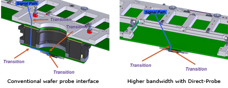
The current industry standard for wafer prober interface (Pogo Tower) degrades the signal quality because the signal must pass through multiple transition points and a distance of 4 to 5 inches. V93000 Direct Probe™ interfaces the test head directly with the probe assembly, reducing the length and number of signal path transitions, maintaining signal integrity.
Mechanically designed for contact force management and planarity to support large surfaces and high pin counts at wafer test
V93000 Direct Probe™ addresses all major contacting challenges (pad probe, Flip Chip, TSV(Through Silicon Vias) and WLCSP) by supporting contact force up to 300 kg and maintaining planarity (1mm over 44,000mm2) for excellent mechanical and electrical contact quality for large die sizes and in high pin count devices such as with MPUs and GPUs.


