Features
The HSM Series leverages the advanced test technology and extended architecture of the proven Advantest V93000 test platform to ensure high test quality and fast "yield learning" at the lowest cost of test in this memory category. Using the proven per-pin timing architecture of the V93000 platform, the HSM Series delivers the functionality to address the most demanding DRAM technologies, including DDR3, DDR4, XDR and GDDR, and provides the flexibility to address the requirements of future DRAM technologies to ensure your test investment is protected.
Proven in R&D and validation labs worldwide, the V93000 HSM is perfect for engineering and design verification with it’s scalable performance?up to 12.8 Gbps with HSM HX?plus compatibility with production systems.
V93000 HSM Platform
Industry leading high-speed memory final test, scalable to 8Gbps, with longest life, superior throughput and lowest cost of test.
The requirements of today’s high-speed memory - higher speeds, performance, production volume - means that test systems must offer greater functionality and parallelism while maintaining low cost of test. The scalable platform architecture of the Advantest V93000 HSM combines functionality, performance and flexibility into a single test system with unmatched overall test economics for outstanding return on investment.
Leveraging the proven per-pin timing architecture and technology components of the V93000 platform, the HSM series features significant architectural extensions addressing the unique requirements for final test of DRAMs, thus becoming a TRUE memory-ATE-per-pin architecture. With the majority of the functionality tightly integrated into the system’s test head, the platform offers superior performance, parallelism, unprecedented scalability and control.
The scalability of the V93000 HSM platform means it is future-ready, offering upgradeability to data rates beyond those of today - true investment protection for DDR3, DDR4 and future DRAM technologies.
Components and Options
| System Infrastructure | V93000 Infrastructure |
| Test-Head Options: | - V93000 Large (64-slot) Test Head
- V93000 Compact (16-slot) Test Head
|
| Memory Test Cards | |
| High-Speed Extension Card | HSM HX |
| Device Power Supplies | DC Scale DPS32 and MS-DPS cards |
| System Controller | High Performance HP-LX Workstation |
| Software | HSM Memory Test Software Bundle |
| Testcell partner products | Custom Test Fixture Boards from TSE, Korea |
Solution
- GDDR5 and XDR Test Solution (HSM6800)
Fastest memory at-speed final test solution of ultra high-speed GDDR5 and XDR, scalable to 8Gbps with superior throughput, yield and lowest test cost. - DDR3 and DDR4 Test Solution (HSM3G)
Economical at-speed mass production test solution for DDR3, DDR4 and beyond with 10-year system lifetime for multiple device generations.
GDDR5 and XDR Test Solution (HSM6800)
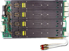
HSM6800
Fastest memory at-speed final test solution of ultra high-speed GDDR5 and XDR, scalable to 8Gbps with superior throughput, yield and lowest test cost
The Advantest V93000 HSM6800 is the fastest memory solution available today, providing scalable performance to 8.0Gbps and superior throughput and yield for low-cost volume production test of ultra high-speed memory devices, including GDDR5 and XDR.
At-speed final test, scalable to 8Gbps
The HSM6800, targeted for volume production test of ultra high-speed memories, offers native 6.8Gbps at-speed I/O and at-speed memory core access testing up to 64-sites GDDR5 in parallel as well as superior accuracy for best device quality and manufacturing yields.
With its unique twin strobe double clocking feature, the maximum test speed can be scaled to an industry leading 8.0Gbps per pin, addressing the future speeds of all available ultra high-speed memory technologies.
Superior throughput and yield for lowest cost of test
The unmatched native speed headroom of the HSM6800, with its unique 8Gbps twin strobe double clocking feature, provides true 64-sites GDDR5 parallel test capability over the full speed range without the typical throughput penalties of traditional double clocking or pin-muxing implementations, attempting to increase the native ATE speed limits. The resulting benefit is an industry leading throughput and yield for up to 2x good devices per hour and lowest cost of test.
Features & Benefits
| Feature | Benefit |
64-sites GDDR5 and XDR at single pass - Native data rate up to 6.8Gbps
- 8Gbps twin strobe double clocking
| Avoids "double clocking" or "pin muxing", provides up to 100% throughput advantage for test speeds beyond 4.0Gbps as well as best test coverage and yield for best-in-class cost of test. |
Memory ATE per-pin - Per pin APG
- Per pin pattern memory
- Per pin PMU
| Fully parallel pattern execution, DC tests and eye-width measurements for best multi-site efficiency. Up to 20% throughput advantage resulting in lowest cost-of-test. |
| Simultaneous Bi-directional (SBD) | At-speed test of I/O pins on a single transmission line without data bus collisions. Full at-speed test coverage, shortest test-times (no padding), lowest cost-of test. |
Complete feature-set: - Jitter Injection & Measurement
- Embedded Parallel Search
- Real-time Strobe Adaptation / Source-Synchronous
- Programmable Signal Equalization
| Ability to test all high-speed failure mechanisms and to ensure high-speed signal integrity Highest test-coverage and yield. |
| Per-pin timing | Recovery of timing margins for highest yields. |
| Lowest Timing Jitter and lowest skew | Repeatable, reliable and accurate timing test for highest yields |
| Most Flexible pin electronics, highest bandwidth | Flexibility to address all high-speed memory technologies. Investment protection |
Programmable at-speed APG per-pin - CRC Data Generation
- ABI / DBI Support
| Enables most complex memory test patterns for any fault algorithm to ensure required test quality and fast yield learning.
Ready to test advanced I/O capabilities of current and next generation memory architectures. |
Key Specifications
| Specification | Value |
| Maximum Test Speed | 8.0Gbps (6.8Gbps native) |
| Example Parallelism | 64-sites GDDR5
256-sites DDR3 |
| Special Functions | - Simultaneous Bi-directional (SBD)
- Real-Time Strobe Adaptation
- Embedded Search Support
- Programmable Signal Equalization
- Jitter Injection & Measurement
- CRC Data Generation
- ABI / DBI Support
|
DDR3 and DDR4 Test Solution (HSM3G)
Economical at-speed mass production test solution for DDR3, DDR4 and beyond with 10-year system lifetime for multiple device generations
The Advantest V93000 HSM3G is the only test solution available today for low-cost volume production of DDR3, DDR4 and beyond. HSM3G offers highly accurate at-speed testing and is scalable to 2.9Gbps. A multi-generation growth path via economical upgrades up to 6.8Gbps date rate provides a unique lifetime value and outstanding return of investment.
Lowest cost of test for mainstream DDR3 & DDR4 up to 2.9Gbps
HSM3G provides highly accurate at-speed I/O and at-speed core access test scalable up to 2.9Gbps, covering the entire DDR3 generation and at least the first two future mainstream speed bins that are expected for DDR4, which are 2.133 Gbps and 2.667 Gbps.
HSM3G achieves native 2.9Gbps data rate, without pin-muxing or double clocking, which guarantees true 256-sites parallel test over the entire speed range without test-time penalties and without compromises to accuracy, functionality, test coverage or yield.
Due to its inherently superior memory ATE per-pin throughput, the V93000 HSM3G provides test-time savings of up to 20 percent. It delivers fully parallel pattern execution, as well as fully parallel DC tests and eye-width measurements, which enables the industry’s best multi-site efficiency. Combined with a competitive price point, the V93000 HSM3G test system provides lowest cost of test for the targeted DRAM speed classes.
Multi-generation test platform with 10 year lifetime via economical upgrades
A unique benefit of the V93000 HSM3G is its future-ready upgradeability to HSM4000 and HSM6800, which gives access to data rates even beyond those of the DDR3/4 generation, featuring investment protection for DDR3, DDR4 and future mainstream DRAM technologies. This ensures more than 10 years of cutting-edge lifetime value over at least three mainstream DRAM device generations and unmatched long-term test economics for outstanding return on investment.
The V93000 HSM platform is future-ready in terms of speed and functionality, offering the most complete feature-set available on the high-speed memory test market. Its programmable at-speed APG per-pin with support for data bus inversion (DBI) and cyclic redundancy check (CRC) data generation enables to test the advanced memory technology features, ensuring best test quality and yield even for the future DDR4 main memory standard.
Features & Benefits
| Feature | Benefit |
| True 2.9Gbps APG and I/O Data Rate on 256-sites DDR3 at single pass | Addresses within one system: - all mainstream DDR3 speed bins
- AND high-end Gamer DDR3
- AND first two mainstream DDR4 volume bins
Avoids "double clocking" or "pin muxing" for best throughput, test coverage and yield. |
| Three performance options available via flexible license upgrade: | Flexibility and scalability in performance and cost, tailor-made to meet test requirements.
Attractive entry price and low upgrade cost. |
| Upgradeable to HSM4000 and HSM6800 via ASIC exchange (upgrade of key speed-binned test-processor components) | Unique 10-year lifetime through cost efficient upgrades covering three device generations, DDR3, DDR4 and future mainstream technologies.
Safest investment: upgradable to 6.8Gbps today. |
Memory ATE per-pin - Per pin APG
- Per pin pattern memory
- Per pin PMU
| Fully parallel pattern execution, DC tests and eye-width measurements for best multi-site efficiency.
Up to 20% throughput advantage resulting in lowest cost-of-test. |
| Simultaneous Bi-directional (SBD) | At-speed test of I/O pins on a single transmission line without data bus collisions.
Full at-speed test coverage, shortest test-times (no padding), lowest cost-of test. |
Programmable at-speed APG per-pin - CRC Data Generation
- ABI / DBI Support
| Enables most complex memory test patterns for any fault algorithm to ensure required test quality and fast yield learning.
Ready to test advanced I/O capabilities of current and next generation memory architectures. |
Key Specifications
| Specification | Value |
| Maximum Test Speed | 2.3/2.5/2.9Gbps (options) |
| Example Parallelism | 64-sites GDDR5
256-sites DDR3 |
| Special Functions | - Simultaneous Bi-directional (SBD)
- Real-Time Strobe Adaptation
- Embedded Search Support
- Programmable Signal Equalization
- Jitter Injection & Measurement
- CRC Data Generation
- ABI / DBI Support
|
Technology
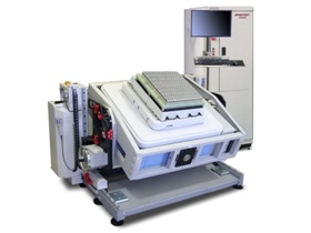
Integrated Test Cell
V93000 HSM Integrated Test Cell
Integrated test-cell maximizes productivity
The V93000 HSM Series comes with an integrated volume manufacturing test-cell, which ensures reliable operation and high uptime as well as efficient one-person operation, comprising tester-to-handler docking, test fixture exchange and test fixture buffer storage within the test-cell for maximized productivity.
- Optimized tester-to-handler docking repeatability
- Flexible floor-plan layout options with small footprint
- Lowest handler index time and cycle time overhead for highest throughput efficiency
- Best temperature accuracy of ±1.5°C or better for best production yields
Engineering and Characterization
Characterization up to 12.8Gbps with best engineering tool-set
Proven in R&D and validation labs worldwide, the V93000 HSM Series provides the industry’s most advanced high-speed memory test capabilities in a cost-effective, small footprint tester, making it a perfect fit for engineering, design verification & characterization.
Due to the scalability of the V93000 HSM platform, the new generation V93000 HSM memory test cards, HSM6800, HSM4000 and HSM3G, are plug-and-play extensions and can be easily combined with already available memory test cards, such as HSM3600 and HSM HX. The ability to upgrade existing engineering test systems with latest generation high-speed technology provides flexible access to higher performance and enhanced high-speed test functionality at lowest capital spending.
- Best in industry high-speed performance scalable up to 12.8Gbps with the market proven HSM HX
- Easy to expand capabilities with new generation memory test cards retaining full compatibility
- Compact Test Head, fully compatible to HVM: same hardware, same software, same DUT boards, same ability to use future platform enhancements
- Easy test program transfer and correlation from engineering to production
- Unique Flexibility, addressing DDR3/4, GDDR5 and XDR within one system
- Best engineering tool-set: Jitter Injection & Measurement, Pattern controlled DC test, Bitmap, Timing Diagram, Real-time Source-Synchronous, Signal Equalization (and more)