 特集 Feature

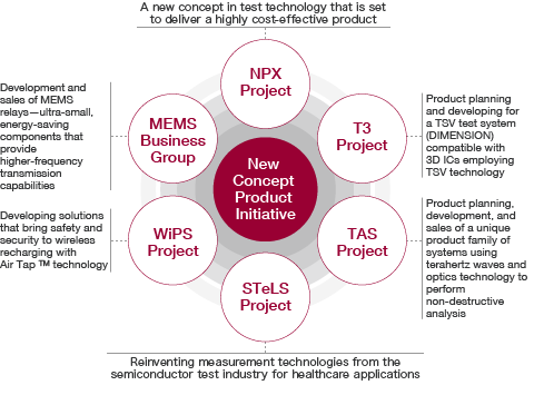
Advantest’s New Concept Product Initiative is chartered to grow the ‘seedlings’ of ideas into new businesses in the medium- to long-term.
Advantest’s New Concept Product Initiative was established in 2009 under the direction of then president Toshio Maruyama, who gave it the mission of generating innovative concepts that would open up new areas of business.
With innovative measurement technologies at the core of our corporate DNA, we are leveraging this expertise to take on the challenge of developing new businesses that go beyond the framework of our existing operations. From this technology-rich starting point, our goal is to expand our reach into cutting-edge fields that play an ever-increasing role in society and effect positive change in the world.
The Initiative’s work is now progressing with six such projects, all independently propagated out of our existing business activities. These early ideas are being nurtured from concept to development in our R&D Department, soon to be rolled out as products that target unmet market needs with cutting-edge technologies.


Kazuo Takano
Leader, T3 Project,
New Concept Product Initiative
Long-awaited 3D stacked ICs utilizing through-silicon via (TSV) wiring techniques are approaching commercialization, and are poised to bring extremely high-performance and multi-functional capabilities to next generation semiconductors. These complex, stacked TSV devices employ a unique fabrication processes and require new testing methodologies for which Advantest is pioneering solutions. In fact, a prototype 3D TSV test system, dubbed DIMENSION, was announced by the company earlier this year. The system integrates a high parallel test cluster along with bare die and 3D die stack automated handling capabilities, which offer improvements to density, power, and performance.
Use of through-silicon via between stacked chips to achieve miniaturization and higher performance in 3D stacked ICs
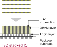
Development of technology for the miniaturization of semiconductors has already reached the stage of studying physical phenomena at the atomic level, and is said to be approaching the limits of what is possible in both physical terms and in terms of development cost. This has led to growing interest in recent years in technology for 3D stacked ICs that package a number of chips together in a vertical stack. This approach has the potential to produce semiconductors with higher performance and greater capacity, without relying on further miniaturization.
A new wiring technology that has attracted attention for its ability to connect these 3D stacked ICs together is called “through-silicon via” (TSV). TSV connects stacked chips together by forming small holes in the chips and injecting conductive metal. Use of TSV allows devices to be made smaller and thinner than is possible using the conventional wire bonding technique that attaches wires to the exterior of a chip.
Another major benefit of TSV devices is that they can minimize problems such as signal delay and attenuation or waveform degradation by connecting circuits on different layers across the shortest possible distance. This makes possible improvements such as faster device operation and lower power consumption because it eliminates the need to increase operating voltage and current to boost drive capacity. Furthermore, the ability to form microscopic, vertical connections anywhere on the chip means that systems can be designed with interconnections numbering in the thousands, increasing circuit layout flexibility, and allowing the development of multi-functional devices that stack different types of semiconductors, such as memory, processors, and image sensors. Even low end semiconductor devices achieve huge advantages using 3D TSV, such as sensors, RF amplifiers and even passive components. Recognizing these advantages, major semiconductor manufacturers and assembly manufacturers are currently working on development of TSV devices.
New testing processes required for mass production of TSV-based devices
As described, TSV devices promise significant advantages over traditional ICs in performance and capacity. However, to enable mass production of these devices, new wafer processing technologies need to be developed in areas such as wafer thinning (to create thin layers to make it easier to bore fine holes), TSV bumping (a process for electrode mounting) and 3D stacking (a process for stacking multiple chips).
TSV device production flow
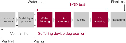
Semiconductor production lines typically perform testing at two different points: wafer testing at the end of the wafer process and final testing after the chips have been diced and packaged. Production of TSV devices, however, involves a number of additional processes that take place between these two tests. Accordingly, to boost yields, it is important to perform additional testing before and after these new processes to confirm device quality, performance and reliability.
Development of handling mechanism able to inspect delicate devices safely and reliably
With the aim of moving TSV device technology forward, Advantest developed the industry's first prototype 3D TSV test system. Dubbed DIMENSION, and exhibited at ADVANTEST EXPO 2012 in June 2012, this integrated solution offers efficient testing to safely and reliably handle device structures not supported by conventional automatic test equipment (ATE), including individual chips formed on extremely thin substrates, and multiple chips that have been fully or partially stacked.
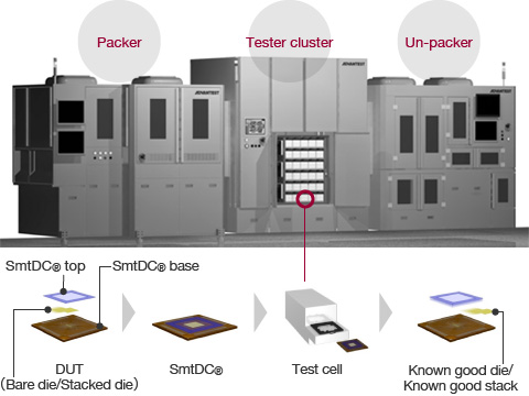
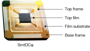
Advantest originally developed the Smart Die Carrier (SmtDCR) that acts as a “Temporary Package” for the safe handling of very delicate devices, including stacked chips or individual chips formed on extremely thin substrates. It works by encasing the devices to be tested in film. Advantest also developed an advanced device handling mechanism incorporating alignment control capable of positioning devices on the carrier with precision of ±10μm or less, which can cope with large numbers of closely spaced pins. For the operations of device transport and encasing, and for the unsealing, sorting and delivery operations performed after testing is finished, this has successfully produced a system able to operate automatically at a speed suitable for mass production.
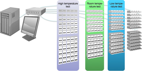
Efficient test process using a clustered test system
Advantest has also employed innovative concepts in the testing process itself. Conventional device testing typically uses a large tester to conduct simultaneous testing of large numbers of chips formed on a wafer, or large numbers of packaged devices. Unfortunately, an unavoidable consequence of this configuration is that it increases the distance between the tester and the devices being tested. TSV devices, however, are designed with a reduced drive capacity compared with conventional devices, making it necessary to reduce, as far as possible, the distance between device and tester during testing. Added to this is the fact that TSV devices have significantly more input and output signals than conventional devices. Consequently, there is a limit to the processing capacity that can be achieved using a test system based on the centralized testing approach that tests multiple devices in parallel.
To overcome this problem, Advantest developed a new highly miniaturized “test cell” that minimizes the distance between device and tester, and which is capable of testing a single device with up to 2,000 pins. By combining large numbers of these test cells into a highly flexible and expandable test cluster, this approach produces a distributed-architecture test system able to efficiently perform the series of tests and processes needed by TSV devices, and to do so with the required processing capacity.
For example, each test cell has a device temperature control function with a range of -20°C to +125°C, and the system incorporates transport robots for moving carriers between test cells. When performing testing at different temperatures, this avoids the need to change temperature settings for each test as occurs in conventional test systems. By controlling test cell temperatures to establish high, medium, and low temperature zones, the same test cluster can perform the different temperature tests simultaneously and efficiently. Naturally, test results from each test cell are collected automatically, and RFIDs can be used to track device and carrier information.
Test cluster
Along with the development of the DIMENSION, Advantest has also built a prototype desktop model called a “personal tester” that contains a single test cell. Because it can be used to develop test programs for the actual production line under the same conditions that occur on the line itself, the personal tester helps shorten turn-around-time (TAT) in semiconductor device development.
Since their announcement, the DIMENSION and personal tester prototypes have provoked considerable reaction from the semiconductor industry. Advantest now plans to proceed with commercialization of these machines, taking into consideration the input generated since the concept was introduced. Advantest intends to continue helping improve the quality and reliability of semiconductor devices by supplying test solutions based on technology that anticipates the industry's direction.

Manabu Kimura
Leader
CloudTesting Service Group

As semiconductors continue to play an ever-increasing and vital role in society, there is a growing need for accessible test solutions to measure and evaluate IC functionality and quality at every stage of the manufacturing process. In addition to design, procurement, and training needs, the need for less traditional cost-effective test solutions in research and at institutions of higher education is also increasing. To address the demands of this expanding segment, Advantest has introduced its CloudTesting™ Service the industry’s first ever on-demand test solution that can meet an ever more diverse set of customer needs.
Meeting the testing requirements of a wider population
Keeping pace with technological progress in chip integration and functionality, Advantest continues to apply a wealth of intellectual property (IP), including test functions and applications software, to the challenge of improving productivity during volume production. The company’s newest large-scale test systems offer I/O pin counts in the 10,000s and unprecedented levels of performance and functionality.
However, Advantest recognizes that even these efficient new large-scale systems cannot meet the testing needs of all customers. As the semiconductor industry evolved from a primarily IDM (Integrated Device Manufacturer) driven business to a broader model that includes foundries, ‘fabless’ design companies and test houses, Advantest has stayed ahead of the trends, designing unique test solutions for diverse customers.
The new CloudTesting™ Service is the company’s latest offering to target the needs of design houses which may lack the resources to invest in ‘big iron’ testers. It is also an optimal solution for large semiconductor manufacturers’ R&D operations, where an average of 25 engineers must currently share a single test system, compromising efficiency and degrading job performance. Offering on-demand “cloud” access to Advantest’s cutting-edge test technology, the CloudTesting™ Service is also an affordable option for universities, research institutes, and training centers, giving students hands-on experience and the freedom to experiment without the capital expense outlay.
An on-demand service that enables customers to freely select functions and software
Advantest’s CloudTesting™ Service gives customers access to cutting-edge test solutions using nothing more than a PC and an internet connection. Proprietary test software (including test applications and evaluation / analysis tools) can be downloaded from the cloud through a dedicated small-size CloudTesting™ Station terminal provided by Advantest to each subscribing customer. This “plug and play” hardware enables the PC to function as an on-demand test environment using precisely calibrated tools. Compared to large-scale testers, throughput is relatively limited, but thanks to Advantest's industry-leading test technology, the CloudTesting™ Station can hold its own against the newest test systems on the market. Most notably, the CloudTesting™ Service requires no upfront investment at all. Customers have the freedom to select and add test functions and applications according to their needs.
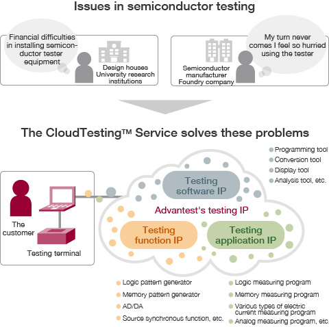

Testing terminal

CloudTesting™ Service web page
A test solution that contributes to sustainable progress in the semiconductor industry
Since introducing the prototype model of its CloudTesting™ Station in 2010, Advantest has conducted customer research among potential users of the device, including global semiconductor manufacturers and distributors, design houses, and universities and research institutes. The company’s research indicates the existence of considerable latent demand for the service. Customer feedback has also been incorporated into the CloudTesting™ Service, such as suggestions that the solution be usable to identify counterfeit products, and requests for troubleshooting functionality.
With all relevant patent applications completed, Advantest is anticipating the official launch of the CloudTesting™ Service in the fall of 2012. The new service exemplifies Advantest’s commitment to provide leading-edge test solutions to an increasingly diverse set of customers, helping to shape a sustainable model for progress in the semiconductor industry.

We expect that the easy-to-use and compact interface will enable use of the CloudTesting™ Service in evaluation of a wide range of actual devices. Going beyond evaluation, we expect it to also contribute to the shortening of test program compilation lead times.
Takashi Maruyama
Chief Specialist
Analog System LSI Test Design Group, Analog System LSI Development Dept.
Analog System LSI Division, TOSHIBA MICROELECTRONICS CORPORATION

Taiichiro Ida
STeLS Project
New Concept Product Initiative

Drawing upon decades of expertise in developing advanced measurement technologies Advantest is now turning its sights on practical applications for new diagnostic technologies in the field of healthcare. One such project is the development of a prototype photoacoustic imaging system that can safely examine damage in skin tissue. This project is being carried out jointly with a well-known medical research institution. Going forward, the Company is aiming to have this prototype certified as a medical device and in concert will be developing new applications for this technology.
Using the photoacoustic effect to safely examine human tissue
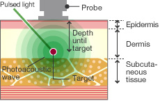
Photoacoustic effect
Since its founding in 1954, Advantest has amassed an impressive range of technologies and expertise in its core field of electronic measurement, and is recognized globally for its cutting-edge products and services, particularly in the field of semiconductor tests. As a means of maintaining its industry leadership, the Company is relying upon its core capabilities to diversify its product lines, and has taken on the challenge of developing innovative testing and diagnostic technologies for the healthcare field.
One such effort is its photoacoustic imaging system now under development. This system relies upon the properties of the “photoacoustic effect,” which is the emission of an ultrasonic(photoacoustic) wave through adiabatic expansion that occurs when pulsed light is directed at and absorbed by a material. This effect is harmless to human tissue yet enables an image to be created to detect the presence of specific elements within the tissue and make visible any changes that have occurred.
For instance, one property of hemoglobin, which is present within the red blood cells of living organisms, is that it absorbs green light. Therefore, when tissue is irradiated with the light of a green wave length, only the hemoglobin generates a photoacoustic wave, through the photoacoustic effect. When this acoustic signal is measured by a sensor and converted into an image, it becomes possible to ascertain conditions in the part that includes the hemoglobin; for example, location of blood vessels and presence of blood flow.
Using proprietary technology to realize highly sensitive and real-time image processing

Prototype photoacoustic imaging system
(not certified as a medical device at present)

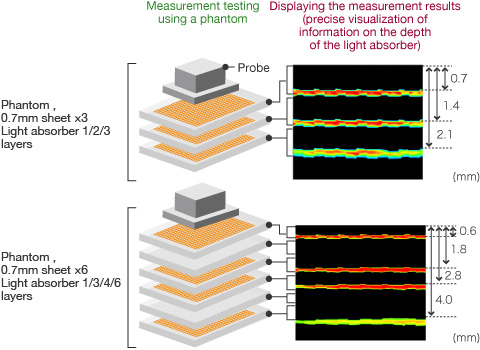
Probe and phantom

Phantom
In June 2010, Advantest began collaborating with a medical research institution which had been developing this new technology for applications in dermatological testing and other areas. Since then, Advantest has developed additional key technologies and systematized testing devices to further this application. In April 2012, the company completed a prototype of the new photoacoustic imaging system (not certified as a medical device at present) that employs a "phantom" to ensure the accuracy of the system. Developed jointly with a leading Japanese research organization, the phantom imaging function enhances performance by periodically checking the output of the imaging system against values generated from the analysis of a plastic sample--known as a phantom--with a probe. (See fig. on the right.) This assures the high quality of images produced by the system.
In photoacoustic imaging, a minute acoustic signal emitted by the target material must be captured and accurately converted into an electrical signal. Advantest has applied a proprietary advanced signal processing technology, originally developed for its measurement business, to this photoacoustic application, in order to realize a multichannel sensor with extremely high levels of sensitivity.
Moreover, ultrafast signal processing and proprietary algorithms allow the system to reconstruct images at a top speed of 30fps (frames per second), which is the same as conventional video imaging. This enables easier examinations, as the images can be observed with no lag, and operators can monitor subjects in real time even while the sensor is being moved.
Furthermore, the large size of the laser light source used in current photoacoustic imaging research makes it difficult to mount it on a device. But Advantest is aiming to enable the device to be both miniaturized and integrated with the laser light source, by developing a new, smaller light source with high-power laser-emitting capacity.
Developing new applications
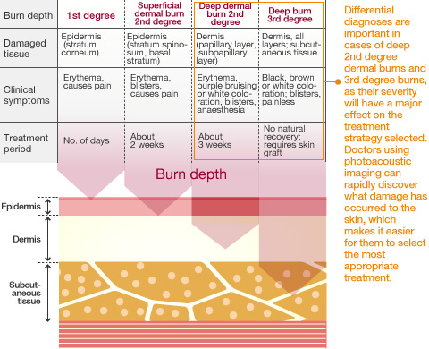
Going forward, after Advantest’s photoacoustic imaging system completes its clinical trials, is certified as a medical device, and is employed at accident and emergency centers, medical staff will be able to rapidly access the state of damaged skin, be it from burns or bruising, and provide appropriate treatment.
In the meantime, Advantest continues to improve upon this device and anticipates that once certified, it will make marked contributions to the field of medicine.
Classification of burn depth
Beyond this, the Company is proactively working to develop its photoacoustic imaging system for use in new diagnostic applications other than for dermatological examinations. It also plans to commercialize this technology not just for use in medical diagnostics, but also as a measurement device for use in life-science research.
Advantest intends to integrate the measurement-related technologies and expertise that it has honed over decades with its other cutting-edge technologies, taking on the challenge of creating innovative new products and solutions that can contribute to the development of society and the field of healthcare.

Tatsuru Orikasa
Power Device
Enabling Group

Amid the rising interest in environmental technology throughout the world, the market is growing for power devices, which are a core technology in electric vehicles (EVs) and next-generation power networks.
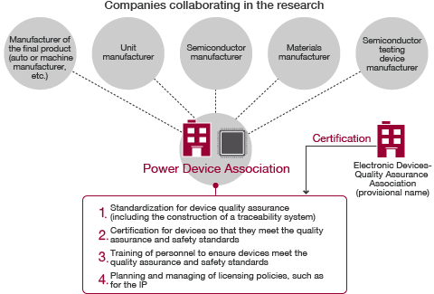
Within the industry, Advantest is championing the cause for standardization of technical specifications and quality inspection methods for power devices, in order to improve overall quality and reliability, and to promote a wider use of these devices industry-wide. It is also independently participating in the Power Device Association, a nonprofit voluntary-membership organization established in 2010, and it is involved not only in efforts to formulate standard specifications, but also in an initiative to introduce an engineer certification system to improve inspection technologies.
A key device supporting the evolution of environmental technology
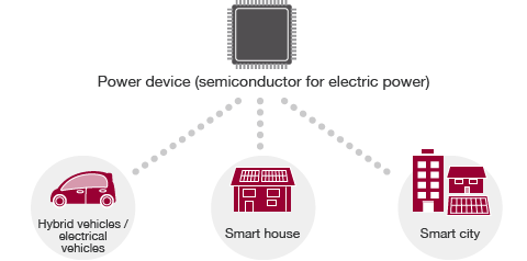
Today, the deteriorating global environment owing to the depletion of energy resources is becoming increasingly more serious the world over. In response, industry and markets are answering the call for a proliferation of eco-sensitive cars, such as hybrid vehicles (HVs) and EVs, and for products for the next generation electric power supply network for smart homes and smart cities. One of the core technologies in these fields of vehicles and electric power is the power device, which is a semiconductor used in electric power transformation and control functions.
The basic principles of operation for power devices are the same as for semiconductor ICs in weak electric current applications, such as those used in memory devices and microcomputers. However, power devices need to be able to regulate higher voltage and current levels. In some cases, they are exposed to an extreme environment, including high temperatures and intense vibration. Moreover, as they are used in mission-critical fields such as vehicles with high safety standards, and the electric power network which is an important part of the social infrastructure, the development of power devices and the production technology used for them must ensure that high levels of quality, reliability and durability are maintained, regardless of their application.
Currently, the Japanese manufacturing industry is the world leader in the development of power devices, their production technology, and the applied technologies for HV/EV and electric power equipment. However, unlike for semiconductors used in weak electric current applications, industry-wide benchmarks for technical specifications and quality control methods have yet to be established. Instead, the auto and equipment manufacturers that use power devices and semiconductor manufacturers have each established their own proprietary quality control standards.
Achieving major quality assurance benefits
Going forward, the Japanese manufacturing industry will continue to provide users throughout the world with power devices and products installed with power devices. In order for these to be used safely and securely, it is important for the industry to establish power device standards based on the intended use, with mechanisms for objective third-party evaluation and authentication of device quality and safety.
Advantest advocates that in the future, when market growth leads to mass production and reduced production costs, the enforcement of industry-wide standard specifications over proprietary standards will benefit the consumer as well as overall safety. Also, from the perspective of quality assurance, once power devices are authenticated as a ‘standardized product’ that have met industry-wide and open technical specifications and have passed verification testing, then society’s confidence in the product will increase.
Moreover, as interest in environmental technology is increasing throughout the world, many of the world’s leading companies in Europe, the United States, and other regions, are paying greater attention to the growing importance of power devices. For the Japanese manufacturing industry to maintain and strengthen its competitiveness in the field in the future, it is vital that it creates at the earliest opportunity standard specifications while also deepening ties with leading overseas companies and seizing the initiative in the formulation of global standards.
With an eye to standardization, promoting technological exchanges and educational activities
For many years, Advantest has supported the quality inspection process for semiconductor devices through its development and supply of semiconductor test systems. The need to create standards for power devices is now accepted as a critical path by the industry at-large. In April 2010, Advantest established an in-company project and began actively promoting standardization to the industry, the government, and other relevant bodies.
As a result of these efforts, in October 2010 the Power Device Association was created, with the members coming from both private and public sector organizations, and from companies in power device-related industries, such as manufacturers of automobiles, equipment, and semiconductors. Since its establishment, the Association has been working toward the standardization of technical specifications and quality-measurement methods for power devices. In addition, it has been promoting the sharing of technological information among its members and conducting educational activities on how to improve the reliability of power devices and the importance of standardization.
The Association has since convened Power Device Seminars in three cities - Tokyo in December 2010, Osaka in June 2011, and Fukuoka in February 2012. It invited experts from industry and public bodies to these meetings, the goal being for the attendees to share information on such topics as market prospects for power drives, the technological issues they face, and the potential of next-generation silicon carbide (SiC) power devices. In addition, in September 2011 and in March and May of 2012, it held its Power Drive Workshop in Nagoya, with the themes of ”Evaluating the Reliability of Power Devices for Vehicles” and ”Improving the Quality of the Next Generation Power Devices (SiC).” Researchers at the leading edge of this field discussed these themes, aiming to discover problem areas and search for solutions.
Role of the Power Device Association
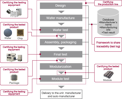
Traceability system (concept)
Introduction of the engineer certification system for improved inspection technology
Going forward, the Power Device Association will continue to strengthen its organizational structure while working to formulate technical and quality assurance standards, the goal being to establish international standards by around 2015. Also, in order to improve the level of power device quality inspections in power-device related industries, it plans to implement its Test Engineer Certification program to support companies’ personnel training. In addition, in cities that are implementing METI’s Project for Promoting the Introduction of Smart Communities, such as Kitakyushu City, Fukuoka Prefecture, it is working with local companies and government bodies participating in this project in order to contribute to the revitalization of regional industry.
Advantest has taken the lead and been involved in the management of the Power Device Association since its establishment. In the future, it will continue to join forces with other member companies and carry out initiatives toward the creation of standards for power devices and to promote the use of products installed with power devices, the primary reasons for the Association’s establishment. In addition, as a test system manufacturer, Advantest will continue to improve the quality and reliability of power devices by rapid development of test equipment that will be compliant with the technical and quality assurance standards that are to be formulated, and also by providing its expertise in measurement technologies.

